
You've probably heard, that it's hard to begin with FPGAs and hardware description languages such as VHDL or Verilog. These languages may need a different way of thinking but a lot of things are actually very easy to implement on an FPGA.
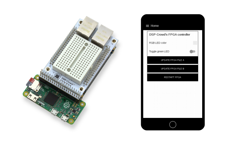
What? You don't believe us? Then let's check out how you can control an RGB-LED using your smart phone and an awesome FPGA board, the DE0 nano.
Overview
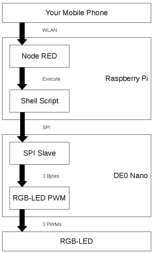
Let's take a look at the overall structure of our little system:
Hardware
The following is needed:
- your smart phone
- a Raspberry Pi
- the DE0 Nano FPGA board
- and an RGB-LED
The following is needed if you want a tidy desk:
- DSP-Crowd's Raspberry Pi to DE0 Nano connector
Software
Every piece of code can be downloaded at our GitHub account DSP-Crowd.
Smart Phone
On your phone you don't have to install anything. The user interface is just a website which is running at port 1880 on the Raspberry Pi. You only need to be able to access your Raspberry Pi via network. We recommend assigning a fixed IP address to the R-Pi. This way you can always use the following web address on your phone:
http://<R-Pi IP-Address>:1880/ui
Node-RED
The web service on the Raspberry Pi is called Node-RED and is installed on the vanilla Raspbian image. Please check out the Node-RED documentation Running on Raspberry Pi to learn how to start the Node-RED service and to install optional packages.
For our example you will need to install the following packages:
Note: Don't forget to restart Node-RED after installing any packages. Otherwise you won't see the provided items
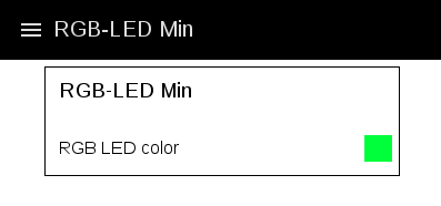
Our interface will look like this:
To create this interface go to the Node-RED editor page:
http://<R-Pi IP-Address>:1880
The editor page looks like this:
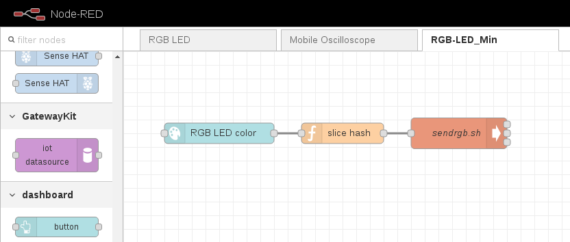
The category dashboard you can see on the left is only visible, if you've installed the mentioned package already. We need three nodes. The first one is called color picker. Grab the color picker node and drag it into the white field. Now the Deploy bottom on the top right corner should be red. This means that something has changed and needs to be deployed. Before you can deploy your changes every node on the sheet must be properly configured. Double click on the color picker node. A configuration dialog appears, where you can edit the label of the node, but in this case everything is optional so you can just press ok. Then press the Deploy button. Now you should see the color picker widget on the Node-RED user interface at:
http://<R-Pi IP-Address>:1880/ui
Every time you interact with the color picker widget it sends the RGB values to it's output. For example #FF0000 (red). We need to send this values to the FPGA. This is done by executing a shell script on your Raspberry Pi with the RGB values as string parameter. But before we can do that, we need to remove the preceding '#'! Otherwise the shell script will not 'see' the parameter.
Grab a function node and insert the following javascript code:
var oMsg = { payload: msg.payload.slice(1) };
return oMsg;
This will remove the first character from the input. Connect the output of the color picker node to the input of the function node.
At this point we've almost finished the Node-RED layer. Our last node is called exec. Double click on the exec node and enter /home/pi/sendrgb.sh as command. And that's it. From now on, every time you interact with the color picker widget on the Node-RED user interface, the RGB values are sent to the shell script.
Note: If something is not working, you can use the debug node to see what's going on
Shell Script
In this layer we have to parse the RGB values from the first parameter and then send it to our FPGA board via SPI. Therefore the script /home/pi/sendrgb.sh must contain the following code:
#!/bin/bash

red=${1:0:2}
green=${1:2:2}
blue=${1:4:2}

echo -ne "\x00\x00\x$red\x$green\x$blue" > /dev/spidev0.3
Parsing the RGB values is quite easy if you use bash as the interpreter for the script. The input is a string with the format 'RRGGBB'. We need to separate the color values and assign them to variables. For this we use the substring function provided by the bash interpreter. The three numbers between the curly braces are interpreted as followed:
- Use parameter 1 (contains 'RRGGBB')
- Start from character 0, 2 or 4. In this case 0 = RR, 2 = GG and 4 = BB
- Use only two characters
Finally we send the RGB values to the FPGA by writing the data with echo into the SPI device.
Note:
- Before you can use an SPI device you have to activate it first. Please check out the official Raspberry Pi documentation about SPI
- In this example we use device ID 0.3. You will probably have to alter this
- Also only in this example, the SPI slave in the FPGA needs two dummy bytes preceding the RGB values
The two dummy bytes are part of a minimalistic protocol. If you want to extend our example you can use this bytes to select different function blocks in your FPGA. Here we will just ignore these bytes in the SPI slave. And that's it on the Shell Script layer.
SPI Slave
Now things get serious. We reached the world of FPGAs! But don't be afraid! Although the VHDL code contains quite a few code lines, only about 100 lines are interesting to us. In order to keep this blog post clear, we don't insert the entire VHDL code. If you want, you can download the code at our GitHub account DSP-Crowd.
First of all let's take a look at the simulation:
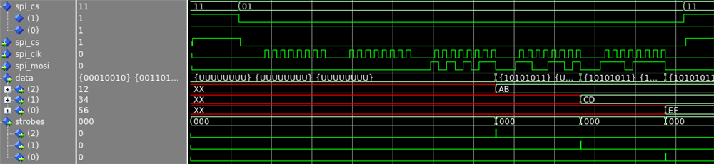
Here we can see, what the SPI slave module must do. On the left side we see the names of the signals in our VHDL design. The signals with the prefix spi are of course the incoming SPI. In this case, the SPI master is the Raspberry Pi and the SPI slave who is just listening on the bus is the FPGA. Because we only send RGB values to the FPGA, we don't need a MISO (Master-In-Slave-Out) signal.
The SPI signals show a typical data transfer. We can see the two dummy bytes and the three RGB bytes containing the hex values 0xAB, 0xCD and 0xEF. The two remaining signals are data and strobes. Unlike the SPI signals, data and strobes are outputs of the SPI slave module.
Note: In our repository we changed the name strobes to valid_bits
The SPI slave module collects all data bits incoming on the SPI at every rising edge of spi_clk. Once 8 bits are collected, the slave module sends a message to the subsequent VHDL modules, the PWM generators. A short pulse on the strobe signal tells each PWM generator, that a certain value (red, green or blue) is valid. At this moment the PWM generators save the value, which is shown in the data signal and use it later on. As mentioned earlier the first two bytes during an SPI transfer are ignored by the slave module.
But how is this achieved? Let's take a look at some code from the SPI slave module (file: spi2rgb.vhd):
proc_comb: process(R, spi_cs, spi_clk, spi_mosi)
begin
	NxR <= R;
	data <= (others => (others => '0'));
	valid_bits <= (others => '0');

	case R.sm_step is
		when SM_WAIT_CS_LOW =>
			if(spi_cs = '0' and R.logging_done = '0')then
				NxR.sm_step <= SM_GET_DATA_BIT;
				NxR.bit_idx <= 7;
				NxR.byte_idx <= 4;
			end if;

		when SM_GET_DATA_BIT =>
			if(spi_clk = '1')then
				NxR.sm_step <= SM_WAIT_CLK_LOW;
				NxR.tmp(R.bit_idx) <= spi_mosi;
			end if;

		when SM_WAIT_CLK_LOW =>
			if(spi_clk = '0')then
				NxR.sm_step <= SM_GET_DATA_BIT;

				if(R.bit_idx = 0)then
					NxR.bit_idx <= 7;

					if(R.byte_idx < 3)then
						data(R.byte_idx) <= R.tmp;
						valid_bits(R.byte_idx) <= '1';
					end if;

					if(R.byte_idx = 0)then
						NxR.logging_done <= '1';
						NxR.sm_step <= SM_WAIT_CS_LOW;
					else
						NxR.byte_idx <= R.byte_idx - 1;
					end if;
				else
					NxR.bit_idx <= R.bit_idx - 1;
				end if;
			end if;

		when others =>
			NxR.logging_done <= '0';
			NxR.sm_step <= SM_WAIT_CS_LOW;
	end case;

	if(spi_cs = '1')then
		NxR.logging_done <= '0';
		NxR.sm_step <= SM_WAIT_CS_LOW;
	end if;
end process;

proc_reg: process(n_reset_async, clock)
begin
	if(n_reset_async = '0')then
		R <= RSET_INIT_VAL; -- This is a comment :>
	elsif(clock'event and clock = '1')then
		R <= NxR;
	end if;
end process;
A process in VHDL is just a piece of digital hardware. It's dependent on the signals which are listed between the parentheses. This list is called the sensitivity list. A process is 'executed' every time when a signal in the sensitivity list changes it's state.
Note: It's very important to add every signal to this list which is read in the process
We have two processes. The one called proc_reg is always the same. It's executed when the reset signal or the clock signal is changed. After the FPGA is configured, the reset signal is held low for a couple of system clock cycles. This causes the registers R to be initialized. After that, the registers R are set to NxR at every rising edge of the system clock.
The process proc_comb is the entire 'brain' of the SPI slave module. It is dependent on the signals R, spi_cs, spi_clk and spi_mosi. Because of R, this process is executed at least every system clock cycle. In VHDL the type of the signal R is called record. It is similar to the type struct in C and other programming languages. R contains all variables we need for our module.
The most important variable is sm_step (SM = State Machine). It contains the information, what the SPI slave module is doing at the current clock cycle. At the beginning, in step SM_WAIT_CS_LOW, the module checks the signal spi_cs at every clock cycle. When the slave module is selected (spi_cs = '0'), the next task for the module is to collect the data bits on the rising edge of spi_clk. This is done in the step SM_GET_DATA_BIT.
After the data bit is collected, it has to be stored in the right place. For this, we have two variables called bit_idx and byte_idx in our record R. Every time 8 data bits are collected (R.bit_idx = 0), they are written to the output signal data. At the same time the appropriate bit in signal valid_bits is set to inform the subsequent PWM generator, that the color value can be used.
RGB-LED PWM
In our last system layer we need to generate the PWM signal for each LED (red, green, blue). Therefore three PWM generators are instantiated. Each generator has two inputs (data_valid and data) as well as one output (led_pwm). In the simulation we see, that the data from the SPI module is stored into the variable R.counter_max. This variable is used in the PWM generators to check how long the output has to be set to high.
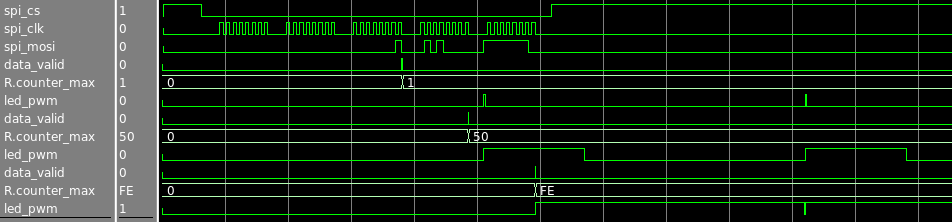
Let's see how we convert the data to a PWM signal (file: byte2pwm.vhd):
proc_comb: process(R, data, data_valid, cnt_strobe)
begin
	NxR <= R;

	if(cnt_strobe = '1')then
		if(R.counter < 254)then
			NxR.counter <= R.counter + 1;
		else
			NxR.counter <= 0;
		end if;
	end if;

	if(R.counter < R.counter_max)then
		led_pwm <= '1';
	else
		led_pwm <= '0';
	end if;

	if(data_valid = '1')then
		NxR.counter_max <= to_integer(unsigned(data));
	end if;
end process;

mainstrobe: entity work.strobe_gen(rtl)
generic map
(
	num_clock_cycles => 50E1 -- 1us strobe
	-- num_clock_cycles => 2 -- Test
)
port map
(
	clock		=> clock,
	n_reset_async	=> n_reset_async,
	strobe_output	=> cnt_strobe
);

proc_reg: process(n_reset_async, clock)
begin
	if(n_reset_async = '0')then
		R <= RSET_INIT_VAL; -- This is a comment :>
	elsif(clock'event and clock = '1')then
		R <= NxR;
	end if;
end process;
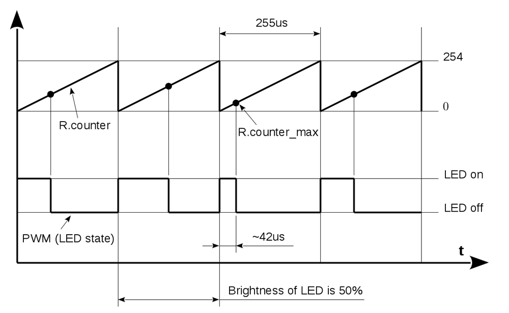
Again we have two processes. The first one, proc_reg, is still the same. In our 'brain' process proc_comb, we have three sections. The first one (line 7-11) increments a counter and resets it as soon as it has reached the value 254. Our counter therefore has 255 steps ranging from 0 to 254.
Section two (line 14-18) actually produces our PWM signal. As long as the counter hasn't reached a certain level (counter_max) the output signal is set to high and the attached LED is on. counter_max thus alters the duty cycle of the PWM. The duty cycle represents the brightness of the LED. Please note, that the process proc_comb is 'executed' every system clock cycle. With a standard system clock frequency of 50MHz, the counter would be incremented every 20 nanoseconds. This would be quite a bit too fast for our LED example.
We can reduce the speed of the incrementation by using a module called strobe generator. This module sets its output for just one clock cycle to high, every time an internal counter reaches the constant value num_clock_cycles. In our example the value 50 is used. Therefore the signal strobe_output is set to high every 1 microseconds (50 * 20 nanoseconds @ 50MHz system clock).
Line 6 in our code assures, that the counter used for the PWM is also incremented only every 1us. This results in a PWM period of 255us (255 counter steps). Following picture illustrates the function of our code:
Summary
And that's it. If you have any question or feedback, please feel free to use the comment section below. If you want to receive similar blog posts in the future, please follow us on Facebook!